Building USoC Part 1: The Wishbone Bus
A few weeks ago, I started researching and outlining a book called The Whole Machine. The goal is to teach teenagers - specifically my son, when he gets a bit older - how to build a computer entirely from scratch.
I don’t mean “understand the concepts.” True understanding only comes from building, which means the goal of the book is to write every single line of code and hardware description from scratch. No massive third-party libraries, no closed-source IP blocks, no hand-waving.
To make it possible for a teenager to actually build a complete machine from the ground up, you have to radically simplify everything. You have to aggressively slice away the historical cruft and unnecessary complexity that plages modern commercial architectures. But a funny thing happened during those first two weeks of conceptual design: I looked at the blueprint and realized it wasn’t just an educational toy. By forcing myself to strip the architecture down to a level where every single line could be built from scratch, I had accidentally designed what I believe is the future of embedded computing.
I immediately shifted gears. Under the moniker AxiomFactory, I am turning that blueprint into a next-generation, WebAssembly-based IoT platform.
While my day job is in software engineering, I am no stranger to formal methods, having verified a small RISC-V core and used Idris to prove distributed Rust algorithms correct about five years ago. Over the last two weeks, I sat down to build and formally verify the first major component of this new SoC: an internal, arbitration-free Wishbone bus fabric.
By leaning on dual-port SRAM and structural simplicity, the design reaches an Fmax of 180MHz on ECP5 and 93MHz on iCE40 - some of the cheapest, most accessible FPGAs on the market. Here is how it works, and how I used Amaranth HDL to formally prove its correctness.
High level design
Our architecture relies on structural simplicity to keep things moving efficiently. To be clear: writing a standard Wishbone bus arbiter is actually quite simple. In fact, I wrote one over the last two weeks just as an exercise. But when looking at the core goals of this SoC, I realized we could bypass traditional bus arbitration entirely.
By utilizing a single UBUS controller and a single RISC-V core as our two Wishbone bus masters, we can build a completely arbitration-free Wishbone bus fabric simply by routing traffic through dual-port SRAM. This post dives deep into this “blue” Wishbone fabric.
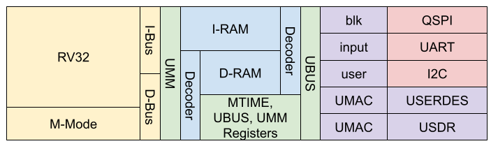
The heart of the SoC is the UBUS, which acts as a specialized DMA (Direct Memory Access) controller. Like a standard DMA, it exposes a set of status and control registers as a Wishbone slave, while using a Wishbone master interface to copy packets directly from D-SRAM to peripheral FIFOs.
By enforcing a strict, unified set of simple peripheral protocols, we can implement a single UBUS driver in kernel space to manage packet queues. This allows us to push the individual peripheral drivers up into WASM user space.
The Standard Wishbone Interface
Before diving into verification, let’s establish the bus protocol baseline. Every System on Chip requires an on-chip interconnect to link its various components together. While options like Avalon or AXI are common, we chose Wishbone because it is exceptionally simple, lightweight, and widely adopted in the open-source SoC community.
In this project, we use Amaranth HDL, a modern, Python-based hardware description language. A standard Wishbone master interface looks like this in Amaranth:
{
  "cyc":   Out(1),
  "stb":   Out(1),
  "we":    Out(1),
  "addr":  Out(addr_width),
  "sel":   Out(data_width // 8),
  "dat_w": Out(data_width),
  "dat_r": In(data_width),
  "ack":   In(1),
  "stall": In(1),
  "err":   Out(1),
}
For a 32-bit bus, the data_width is 32 and the addr_width is typically 30 because data is accessed in whole 4-byte words. (In 64-bit designs, the address width is often artificially capped at a lower value to save routing resources).
How Data Moves on the Bus
When the CPU executes a load instruction (like lb, lh, lw) from I-RAM it, it drives the target address onto addr and expects data back on dat_r. Even though the bus always returns a full 32-bit word, the CPU automatically masks out and discards the bytes it doesn’t need for smaller byte or half-word instructions.
For store instructions, the master sets the we (write-enable) signal high. It uses the sel (byte-select) lines to tell the slave exactly which bytes in the word it wants to overwrite.
If a slave is busy and cannot immediately accept a request, it holds the stall line high. Once the slave successfully processes a transaction, it drives the ack (acknowledge) signal. The master initiates a transaction cycle by asserting cyc, and uses stb to indicate that a valid data transfer is actively being requested on the current clock cycle.
The classic Wishbone specification also includes an err line, which a bus decoder uses to signal a fault if an address is invalid. We removed this signal from our peripherals. Instead, invalid address faults are wired directly from our decoder to the RISC-V mstatus and mcause registers. This keeps our peripherals simpler and saves us from forcing every slave to dedicate a flip-flop just to drive err low.
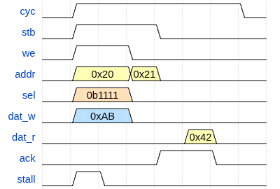
The diagram below illustrates a typical pipelined transaction: a Whishbone write immediately followed by a read within the same cycle envelope.
-
Transaction Start: The master starts the transaction by asserting
cycalong with the write parameters (stb,we,addr,sel,dat_w). -
The Stall: The slave asserts
stallimmediately, forcing the master to hold its signals steady. -
Write Accepted: On the next clock edge, the slave drops
stall, accepting the write phase. -
Pipelined Read: The master immediately transitions into a read cycle by changing
addrand droppingwewhile keepingstbhigh. -
Delayed Acknowledge: Because this slave takes two cycles to process reads and writes internally, the write completion
ackappears a cycle late, followed immediately by the read’sackand valid data ondat_r. -
Transaction Complete: Finally, the master terminates the transaction by dropping
cyc.
To summarize this behaviour mathematically:
- A transaction phase begins when:
cyc & stb & ~stall - A transaction phase completes when:
cyc & ack
Formally Verifying the Interconnect
Now that we understand how data moves, we can establish the formal properties required to prove our Wishbone masters and slaves behave correctly.
The core rule of formal verification is simple: outputs are asserted, inputs are assumed. Because of this, the formal properties of a master and a slave are exact mirror images. Every rule the master must assert as an invariant is assumed by the slave, and vice versa.
Rule 1: Power-On Reset Invariant
This rule ensures the bus starts in a clean, inactive state immediately after reset. No transaction should be active (cyc and stb must be false), and we assume the slave is not issuing a response.
initial = Signal(init=1)
m.d.sync += initial.eq(0)

with m.If(initial):
    m.d.comb += [
        Assert(~self.cyc),
        Assert(~self.stb),
        Assume(~self.ack),
        Assume(~self.stall),
    ]
Rule 2: Transaction Envelope
The strobe signal (stb) must never float high out of nowhere; it can only be asserted inside an active transaction window.
with m.If(self.stb):
    m.d.comb += Assert(self.cyc)
Rule 3: Pipelined Stability Property
If the master attempts a transfer and the slave stalls, the master cannot change its mind or alter the payload. It must hold stb, addr, we, dat_w and sel prefectly stable until the stall clears or abort the transaction.
past_cyc   = Signal()
past_stb   = Signal()
past_stall = Signal()
past_addr  = Signal(len(self.addr))
past_we    = Signal()
past_dat_w = Signal(len(self.dat_w))
past_sel   = Signal(len(self.sel))

m.d.sync += [
    past_cyc.eq(self.cyc),
    past_stb.eq(self.stb),
    past_stall.eq(self.stall),
    past_addr.eq(self.addr),
    past_we.eq(self.we),
    past_dat_w.eq(self.dat_w),
    past_sel.eq(self.sel)
]

with m.If(past_stb & past_stall & ~initial):
    m.d.comb += [
        Assert(self.stb),
        Assert(self.addr  == past_addr),
        Assert(self.we    == past_we),
        Assert(self.dat_w == past_dat_w),
        Assert(self.sel   == past_sel),
    ]
Rule 4: Anti-Spurious Response
A slave must never issue an acknowledgment if there are no outstanding requests on the bus. We keep track of in-flight requests using a simple counter.
outstanding = Signal(8)
req_issued = self.cyc & self.stb & ~self.stall
res_rcvd   = self.cyc & self.ack

with m.If(~self.cyc):
    m.d.sync += outstanding.eq(0)
with m.Else():
    m.d.sync += outstanding.eq(outstanding + req_issued - res_rcvd)

with m.If(outstanding == 0):
    m.d.comb += Assume(~self.ack)
Avoiding Formal Pitfalls
Formal verification is full of subtle traps. One major pitfall is under-constraining the model, where the solver passes your assertions simply because inputs are left floating or dead. When verifying our master we must allow the slave inputs to take any valid sequence of values to truly stress-test the design:
m.d.comb += [
    self.ack.eq(AnySeq(1)),
    self.stall.eq(AnySeq(1)),
    self.dat_r.eq(AnySeq(32)),
]
Another pitfall is trying to prove liveness (that something eventually happens). Liveness properties can be incredibly difficult or impossible to resolve cleanly in bounded model checking. Instead, we convert liveness into a bounded safety property: we verify that the slave responds within a strict timeout window.
Rule 5: Bounded Response Timeout
timeout_count = Signal(2)
with m.If(~self.cyc | self.ack | (~self.stall & self.stb)):
    m.d.sync += timeout_count.eq(0)
with m.Else():
    with m.If(outstanding > 0):
        m.d.sync += timeout_count.eq(timeout_count + 1)
m.d.comb += Assume(timeout_count < 2)
Rule 6: Bounded Request Timeout
with m.If(~self.stb & outstanding == 0):
    m.d.comb += Assert(~self.cyc)
The final major pitfall is vacuity - a state where your assertions pass simply because the logic path is never actually triggered by the solver. To prove our logic isn’t just passing vacuously, we use a coverage statement to force the engine to prove that full pipelined transactions can actually occur under our rules.
Rule 7: Pipelined Transaction Coverage
m.d.comb += Cover(self.cyc & self.stb & self.ack)
Following the verification of a single Wishbone interface, the next phase involves connecting components to build a complete System on Chip. Part 2 will detail the assembly of these blocks, focusing on using a central decoder and dual-port memory to achieve high (F_{max}) on low-cost FPGAs.